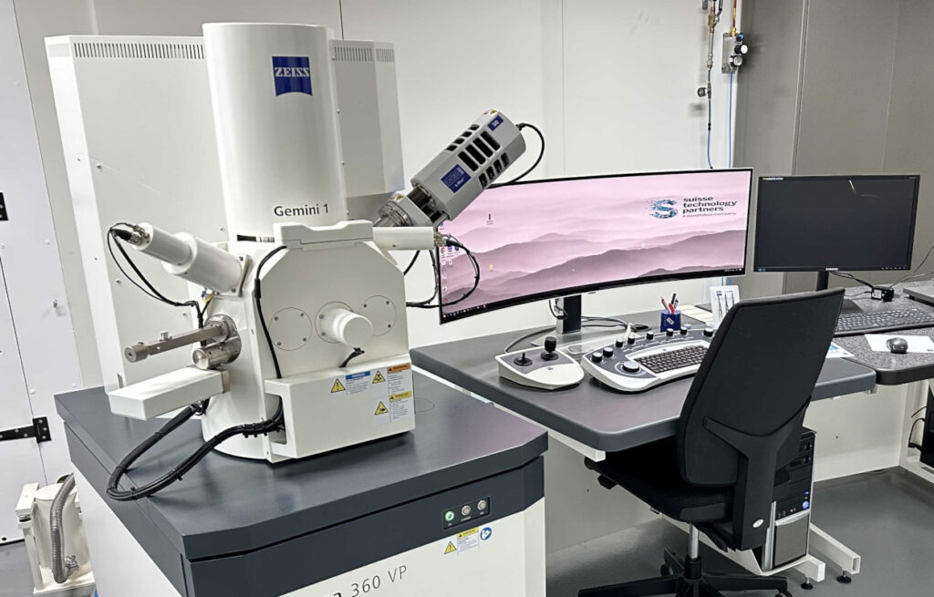
What is a scanning electron microscope – SEM
The abbreviation SEM stands for scanning electron microscope or scanning electron microscopy. The German abbreviation for this is Rasterelektronenmikroskopie or Rasterelektronenmikroskopie. Scanning electron microscopy is a method for high-resolution imaging of surfaces. The SEM uses electrons for imaging, similar to the way a light microscope uses visible light. The advantages of SEM over light microscopy include a much higher magnification (> 100,000x) and a greater depth of field of up to 100 times that of light microscopy. Qualitative and quantitative information for chemical analysis is also obtained using an energy-dispersive X-ray spectrometer (EDS) in conjunction with the SEM (see EDS below).
If the magnification of the light microscope is no longer sufficient, a scanning electron microscope is used.
Scanning electron microscope – operating principle
The SEM produces a beam of incident electrons in an electron column above the sample chamber. The electrons are generated by a thermal emission source, such as a heated tungsten cathode, or by a field emission cathode. The energy of the incident electrons can be 100 eV or up to 30 keV, depending on the evaluation objectives. The electrons are directed through a series of electromagnetic lenses in the SEM column to form a small beam in the SEM column.
Scanning coils at the end of the column direct and position the focused beam onto the sample surface. The electron beam is scanned across the surface in a raster pattern to form an image. The beam can also be focused to a single point or scanned along a line for X-ray analysis. The beam can be focused to a final probe diameter of only about 1 nm (10 Å).
Incident electrons cause electrons to be emitted from the sample due to elastic and inelastic scattering processes at the sample surface and in the near-surface material. High-energy electrons ejected by an elastic collision of an incident electron, typically with a sample nucleus, are referred to as backscattered electrons. The energy of the backscattered electrons is comparable to that of the incident electrons. The lower-energy electrons emitted by inelastic scattering are referred to as secondary electrons. Secondary electrons may result from collisions with the nucleus in which significant energy loss occurs, or from the ejection of loosely bound electrons from the sample atoms. The energy of the secondary electrons is typically 50 eV or less. To create a SEM image, the incident electron beam is scanned in a raster pattern across the sample surface. The emitted electrons are detected by an electron detector for each position in the scanned area. The intensity of the emitted electron signal is displayed as brightness on a cathode ray tube (CRT).
By synchronizing the CRT scan with the scan of the incident electron beam, the CRT display shows the morphology of the sample surface scanned by the beam. The magnification of the CRT image is the ratio of the size of the image display to the sample area scanned by the electron beam.
Two main types of electron detectors are used for SEM imaging.
Scintillator (Everhart-Thornley) detectors are used for secondary electron imaging. This detector is biased with a positive voltage to attract electrons to the detector and enhance the signal-to-noise ratio. Backscattered electron detectors can be scintillator types or solid state detectors.
A moderate vacuum is maintained in the SEM column and the sample chamber so that the electrons can travel unimpeded from the electron beam source to the sample and then to the detectors. High resolution imaging is performed in the chamber at a higher vacuum, typically from 10-5 to 10-7 mmHg. Imaging of non-conductive, volatile and vacuum-sensitive samples can be performed at higher pressure.
SEM resolutions
In a scanning electron microscope, a focused beam of electrons is fired at a sample. The surface is scanned in a vacuum. A resolution of 50 nanometers (1000 nm: 1 µm) can be achieved (magnification at the SEM is 150,000x and more). By comparison, an optical microscope can achieve a resolution of one micrometer (thousandth of a millimeter) (magnification up to 1,000x on an optical microscope).
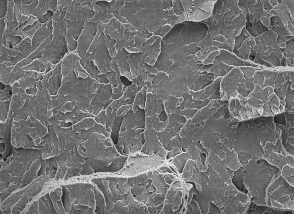
The following scanning electron microscope images show the same object at different resolutions.
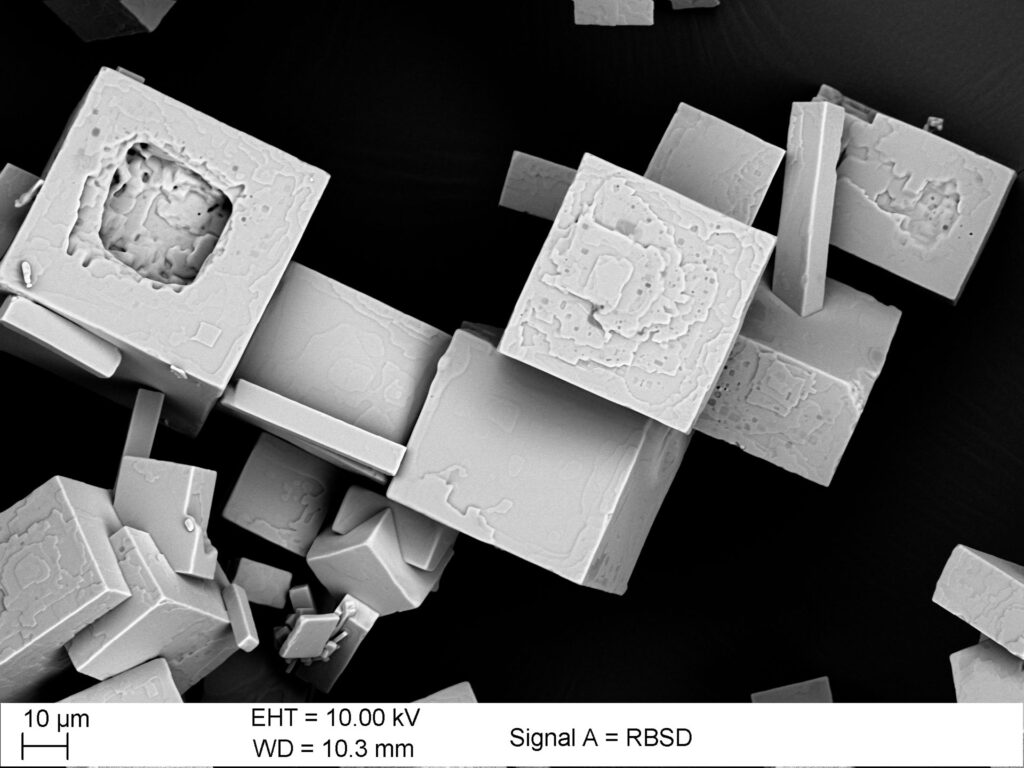
ANALYTICAL INFORMATION
secondary electron image
This mode provides high-resolution imaging of fine surface morphology. Inelastic electron scattering, which results from the interaction between the electrons of the sample and the incident electrons, leads to the emission of low-energy electrons from the vicinity of the sample surface. The topography of the surface features influences the number of electrons that reach the secondary electron detector from each point of the scanned surface. This local variation in electron intensity produces the image contrast that reveals the surface morphology. The resolution of the secondary electron image for an ideal specimen is about 3.5 nm for a tungsten filament electron source SEM or 1.5 nm for a field emission SEM.
backscatter electron imaging
This mode provides image contrast that is composition dependent. Backscattered electrons are produced by the elastic interaction between the sample and the incident electron beam. These high-energy electrons can emerge from a much deeper layer than secondary electrons, so the surface topography is not resolved as well as with secondary electrons. The production efficiency for backscattered electrons is proportional to the average atomic number of the sample material, resulting in compositional contrast, i.e., the backscattered electron image of a higher-Z metallic powder material appears brighter than that of a lower-Z material in a fractured surface containing spherical silica particles. The optimum resolution for
backscattered electron image is about 5.5 nm.
SEM with variable pressure
Traditionally, a conductive specimen or a continuous conductive surface film is required for the SEM so that the incident electrons can be diverted from the specimen surface to the ground. When electrons accumulate on a non-conductive surface, the charge accumulation causes the electron beam to diverge and degrades the SEM image. In variable pressure SEM, a small amount of air is admitted into the specimen chamber, and the interaction between the electron beam and the air molecules produces a cloud of positive ions around the electron beam. These ions neutralize the
negative charge of electrons that collect on the surface of a non-conductive material. SEM imaging can be performed on a nonconductive sample if the chamber pressure is maintained at a level where most electrons reach the sample surface, but enough gas molecules are present to ionize and neutralize the charge. The variable pressure SEM is also suitable for examining samples that are incompatible with high vacuum.
field emission SEM (FEREM)
SEMs that use a thermal emission source (such as a tungsten filament) to generate the electron beam are generally adequate for most samples and provide satisfactory resolution at magnifications up to about 100,000x. However, for high-resolution, high-magnification images, a cold field emission (FE) gun provides the best resolution available to the SEM. The cold FE gun extracts electrons from the FE cathode by applying a strong electric field near a very sharp tip. This method of electron extraction results in a higher electron yield and a smaller beam size, producing a brighter signal with better resolution. Useful magnification for FESEM imaging extends up to 500,000X. A second advantage of FESEM is that high resolution imaging can be performed at very low accelerating voltages. At low voltage, very fine features can be observed more easily and many non-conducting materials can be examined without a conductive coating. Low-voltage FESEM examination is ideal for imaging nanomaterials, polymers and thin films.
quantification
Image magnification is calibrated against a reference standard. Lateral feature dimensions can be easily quantified to better than 0.1 µm. Computer analysis of images can quantify area or volume fractions, as well as particle shape and size.
Examples of applications of a scanning electron microscope
Since a SEM can display images at extreme magnification, the possibilities offered by a SEM are independent of industry and technology. Since grain sizes can be determined at resolutions of up to 150,000x, as can small molecules, it is a widely applicable tool that we cannot do without.
Electron microscopy for technical safety
Our technical safety customers appreciate the possibilities offered by a SEM, for example, to analyze the influence of heat treatment on the microstructure of the material. In damage analysis, grain size determination can also be used to find clues to the cause of damage and to characterize fractures. This is unique in Switzerland in combination with methods x and y and the expertise of our technical safety experts.
Find out more about our expertise in the field of technical safety.
Electron microscopy for aluminum surfaces
With a SEM, for example, the surface condition after anodizing can be assessed. But a SEM can also be used to assess the performance of a degreaser by comparing the contamination on the surface.
Find out more about our expertise in the field of aluminum surfaces
Electron microscopy for pharma and chemistry
Our pharmaceutical experts use the REM to identify the presence of certain small particles.
Find out more about our expertise in the field of chemicals and pharmaceuticals.